
Often when assessing an embedded system, changes can occur (intended or otherwise) that cause the target system to enter a state where it no longer works ('bricked'). In some cases fixing the target is as simple as performing a "factory reset", others may be slightly more involved and require flashing the target using a debug interface (JTAG/SWD/*) or manually flashing an external storage device (SPI/NOR/Nand/eMMC). This post walks through resolving a situation where a target has been 'bricked' with a creative methodology.
During some downtime, I was poking at an off the shelf consumer router that was using Common Firmware Environment (CFE) as a boot loader. While interacting with the CFE trying to identify arguments that are passed to the target's operating system at boot, the system configuration was accidentally corrupted:
CFE> b
Press:  <enter> to use current value
        '-' to go previous parameter
        '.' to clear the current value
        'x' to exit this command
94908AC5300R               ------ 03
94906REF                   ------ 07
GT-AC2900                  ------ 08
Board Id                          :  8  X     <---- whoops
Number of MAC Addresses (1-64)    :  10  ^C   <---- more whoops
x
Memory Configuration Changed -- REBOOT NEEDED <---- whoops saved.
flow memory allocation (MB)       :  14  ----
At this point I figured a final save/write would be required to commit the accidental changes, so I opted to just power cycle the device to avoid making permanent changes. After power cycling the device, an error occurred:
Shmoo WR DM
WR DM
   0000000000111111111122222222223333333333444444444455555555556666666666
   0123456789012345678901234567890123456789012345678901234567890123456789
00 ------++++++++++++++++++++++++++X+++++++++++++++++++++++++++----------
01 --+++++++++++++++++++++++++X++++++++++++++++++++++++++----------------
02 X---------------------------------------------------------------------
03 X---------------------------------------------------------------------
MEMSYS init failed, return code 00000001
MEMC error:  0x00000000
PHY error:  0x00000000
SHMOO error:  0x10c00000
 0x00000082
 0x00000000
When the device came back up, it immediately produced the previous error and failed to enter the CFE. Without being able to access the boot loader, the configuration could not be changed and the boot loader's recovery process could not be utilized either. Searching online for this error was not helpful and resulted in dead ends and the general consensus is if you corrupt CFE in this manner - the device is 'bricked'. At this point I switched to working with my backup device (always have a backup) so I could answer my original question regarding interesting target arguments. As an aside, the setting kernp mfg_nvram_mode=1 mfg_nvram_url=BADURL is particularly interesting.
Later on I circled back to the bricked unit to identify a path to fix it. The target is using a Broadcom SoC and an unpopulated header was found to provide JTAG access:
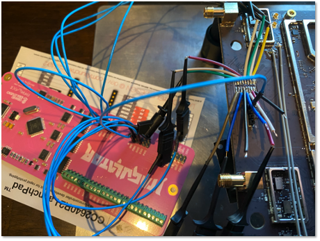
After enumerating the JTAG pinout on the unpopulated header with a JTagulator, it was possible to confirm access using OpenOCD:
$ openocd -f ../interface/jlink.cfg -f bcm49.cfg
Open On-Chip Debugger 0.11.0-rc2+dev-gba0f382-dirty (2021-02-26-14:07)
Licensed under GNU GPL v2
For bug reports, read
http://openocd.org/doc/doxygen/bugs.html
DEPRECATED! use 'adapter speed' not 'adapter_khz'
Info : Listening on port 6666 for tcl connections
Info : Listening on port 4444 for telnet connections
Info : J-Link V10 compiled Dec 11 2020 15:39:30
Info : Hardware version: 10.10
Info : VTarget = 3.323 V
Info : clock speed 1000 kHz
Info : JTAG tap: bcm490x.tap tap/device found: 0x5ba00477 (mfg: 0x23b (ARM Ltd), part: 0xba00, ver: 0x5)
Info : JTAG tap: auto0.tap tap/device found: 0x4ba00477 (mfg: 0x23b (ARM Ltd), part: 0xba00, ver: 0x4)
Info : JTAG tap: auto1.tap tap/device found: 0x0490617f (mfg: 0x0bf (Broadcom), part: 0x4906, ver: 0x0)
Info : JTAG tap: auto2.tap tap/device found: 0x0490617f (mfg: 0x0bf (Broadcom), part: 0x4906, ver: 0x0)
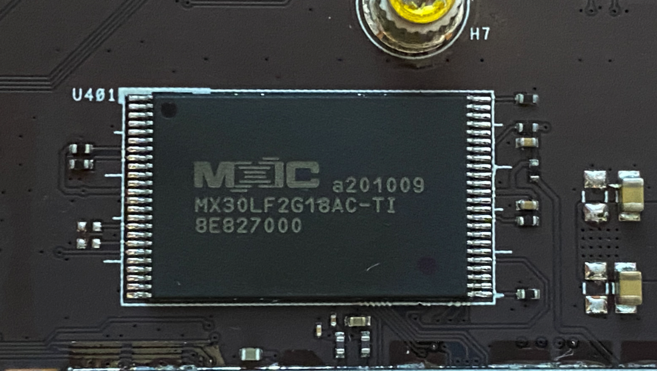
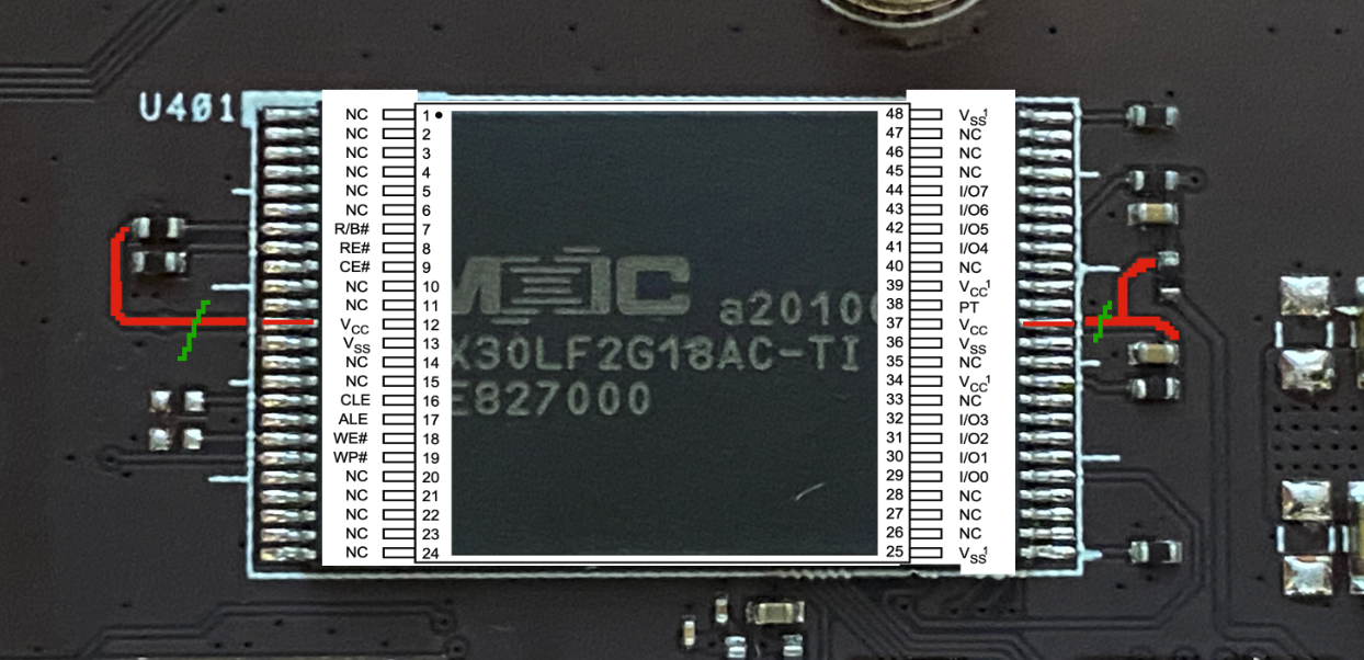
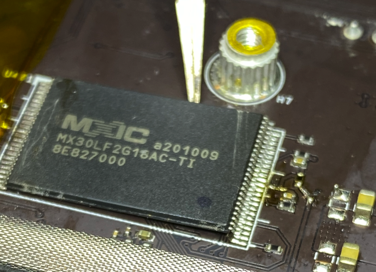
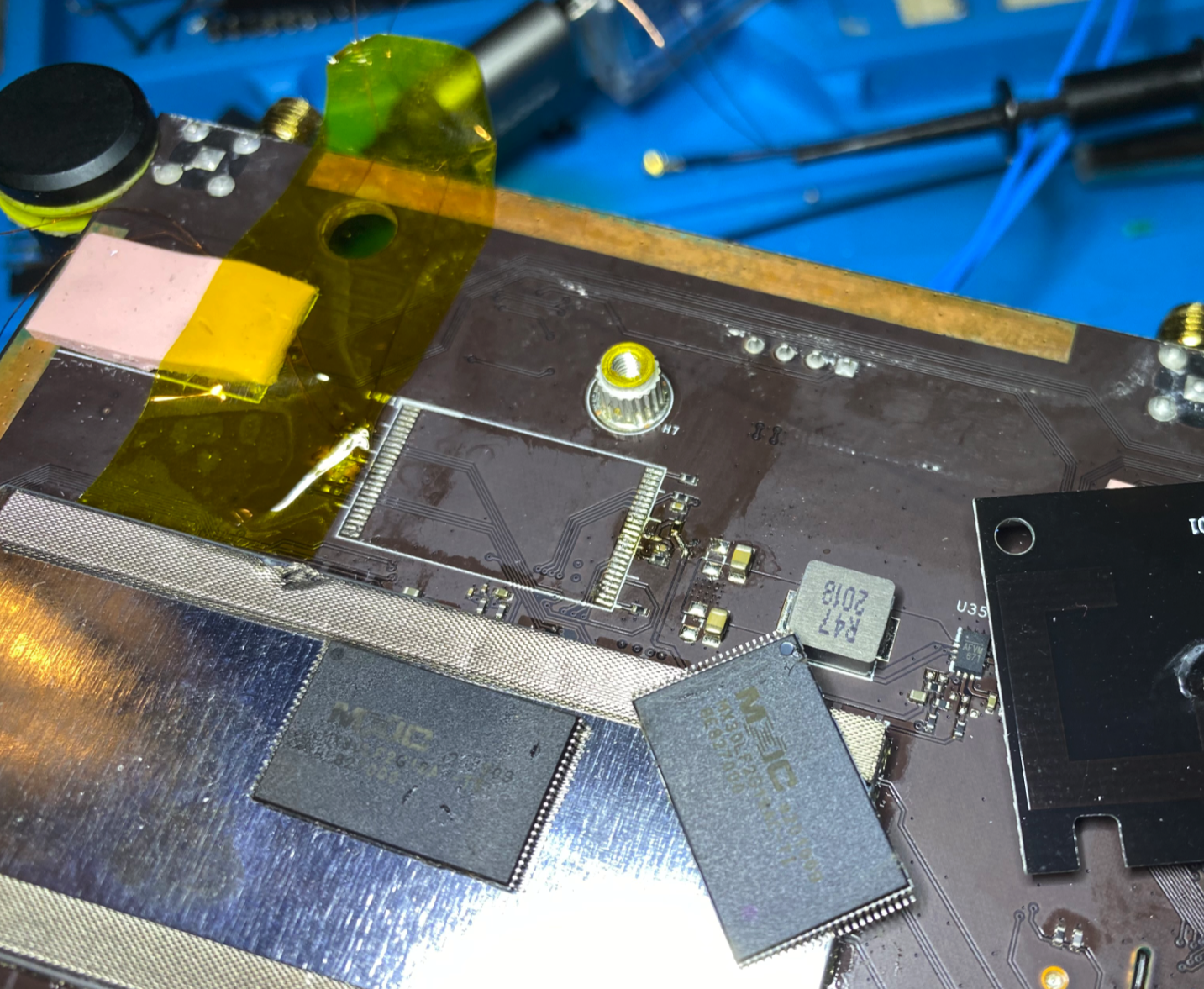
Info : bcm490x.a53.0: hardware has 6 breakpoints, 4 watchpointsThe other path for restoring the system is through the storage device, a Macronix NAND chip:
At this point I started to wonder about something, I still had a working device that I could boot into the boot loader - would it be possible to swap the NAND chip on a running device and use it to flash the corrupted NAND?
Before attempting anything, I asked a co-worker if he thought this stupid idea would have any chance at working, he wasn't optimistic on the outcome (to be fair, I wasn't either) - we made a bet on the results and I went to work.
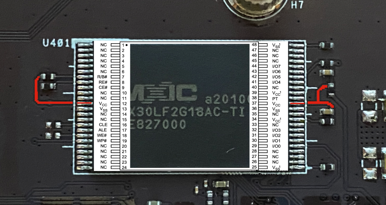
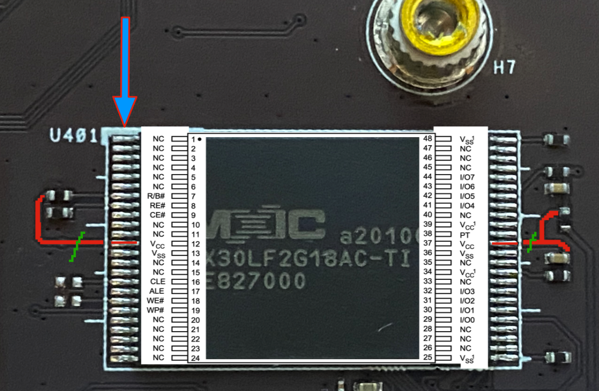
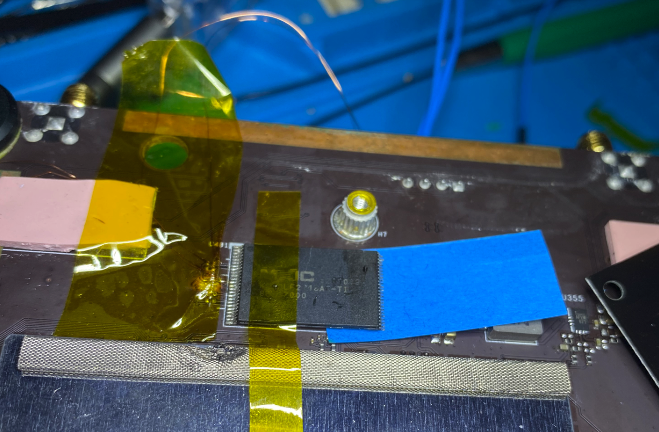
The first stage of testing was to find out if the system would tolerate having the NAND 'removed' while running? I knew that answering this question I would need to be more methodical than just hitting the unit with hot air while its running and removing the chip. The first stage of this process was to identify how the NAND is being powered. The layout looks like VCC is tied into the chip in the following locations:
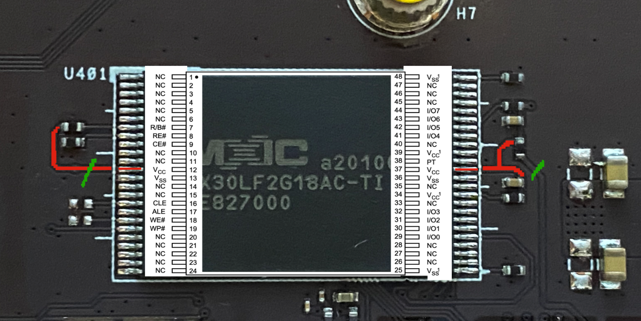
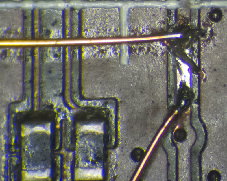
With the VCC lines identified, the easiest way to answer our first question would be to remove the VCC lines from the NAND while the system is running. In order to do this, my first try was to cut the VCC lines and add 'jumper' wires (36 AWG Magnet Wire is great stuff) that can be disconnected once the boot loader is done:
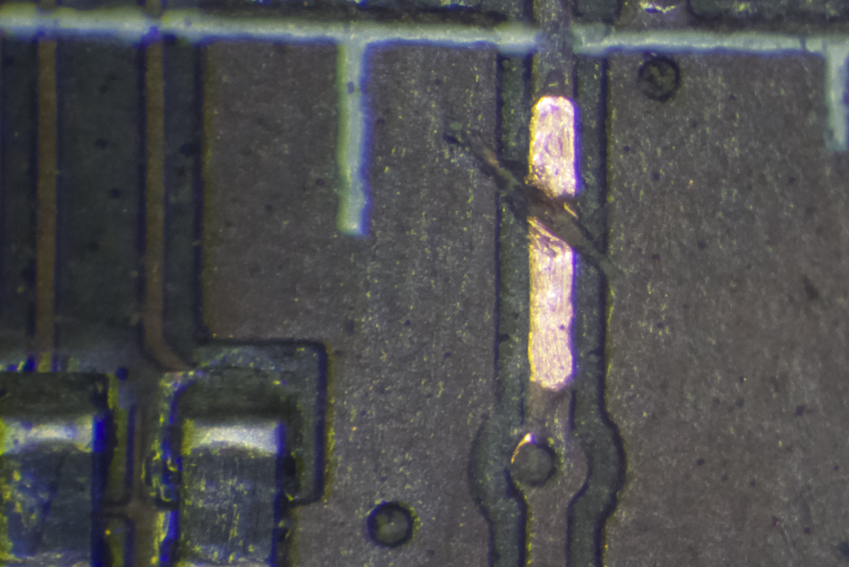
On the right hand side I chose to cut further back on the power trace thinking it would be a better spot as it feeds into a few pins on the NAND. On the first jumper install I used a fiberglass scratch pen to remove the coating and expose the copper and a small knife to cut the trace:
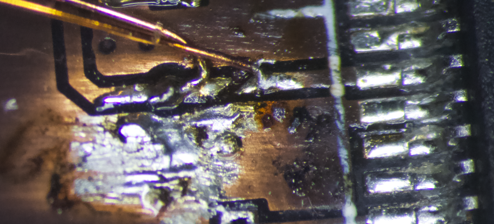
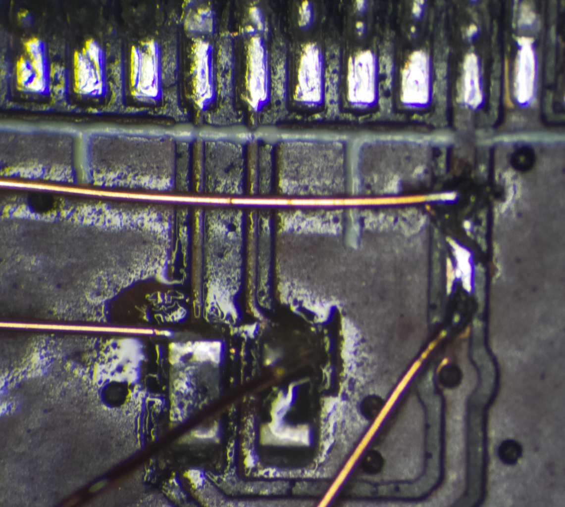
The result was gross as the scratch pen tip was far too big and I ended up exposing lots of copper. Don't use a scratch pen, just a fine tipped knife so you don't end up with a mess. More like this:
With the 'jumpers' installed and connected, the target was powered up to the boot loader (CFE) and the command dn (dump nand) was used to ensure the NAND was accessible, power was then removed by disconnecting the jumper wires:
CFE> dn
------------------ block: 0, page: 0 ------------------
00000000: 00000000 00000000 00000000 00000000    ................
00000010: 00000000 00000000 00000000 00000000    ................
00000020: 00000000 00000000 00000000 00000000    ................
<CUT FOR LENGTH>

----------- spare area for block 0, page 0 -----------
00000800: ff851903 20000008 00fff645 c2b9bf55    .... ......E...U
00000810: ffffffff ffffffff ffee9423 4ba37819    ...........#K.x.
00000820: ffffffff ffffffff ffee9423 4ba37819    ...........#K.x.
00000830: ffffffff ffffffff ffee9423 4ba37819    ...........#K.x.

*** command status = 1
CFE>
web info: Waiting for connection on socket 1.␛[J
CFE>
web info: Waiting for connection on socket 0.␛[J
CFE> ␀----       <----- VCC Removed (reboot)
When the power was removed (marked with 'VCC Removed') the target rebooted and failed to return to the boot loader as the NAND was not accessible. The source of the problem was the right side power cut was in a spot that removed power from the SoC as well as the NAND. Keeping it simple, the initial cut was restored and only the trace closest to the NAND was cut and jumpered:
Bringing the system back up and attempting the previous test gave me the answer to my initial question: when the power is removed by disconnecting the jumper wires, the system remains operational, as confirmed by running the dn command:
<----- NAND VCC Removed
CFE> dn
------------------ block: 0, page: 2 ------------------
Status wait timeout: nandsts=0x30000000 mask=0x80000000, count=2000000
Error reading block 0
00001000: 00000000 00000000 00000000 00000000    ................
<CUT FOR LENGTH>
Status wait timeout: nandsts=0x30000000 mask=0x80000000, count=2000000
----------- spare area for block 0, page 2 -----------
00000800: 00000000 00000000 00000000 00000000    ................
00000810: 00000000 00000000 00000000 00000000    ................
00000820: 00000000 00000000 00000000 00000000    ................
00000830: 00000000 00000000 00000000 00000000    ................
Error reading block 0
*** command status = -1      <----- Expected error reading NAND
CFE>
CFE>
CFE>
<----- NAND VCC Enabled
CFE>
CFE> dn
------------------ block: 0, page: 3 ------------------
00001800: 00000000 00000000 00000000 00000000    ................
00001810: 00000000 00000000 00000000 00000000    ................
<CUT FOR LENGTH>
----------- spare area for block 0, page 3 -----------
00000800: ffffffff ffffffff ffee9423 4ba37819    ...........#K.x.
00000810: ffffffff ffffffff ffee9423 4ba37819    ...........#K.x.
00000820: ffffffff ffffffff ffee9423 4ba37819    ...........#K.x.
00000830: ffffffff ffffffff ffee9423 4ba37819    ...........#K.x.
*** command status = 1      <----- Successful NAND read
CFE>
By confirming it is possible to 'turn off' the NAND on the running system without disrupting the boot loader, the next step was to try to power down the NAND and physically remove it from the board while it's running.
Using hot air and tweezers, one side was lifted at a time (right side then left):
This process resulted in the system restarting and failing to enter the boot loader:
CFE> ␀----    <----- NAND Removed (reboot)
BTRM
V1.6
CPU0
L1CD
MMUI
MMU7
DATA
ZBBS
MAIN
OTP?
OTPP
USBT
NAND
IMG?
FAIL
␀----         <----- FAIL boot loop
Since I had lifted the NAND off one side at a time while monitoring the console it was easy to see that the reboot occurred when lifting the "left" side of the NAND:
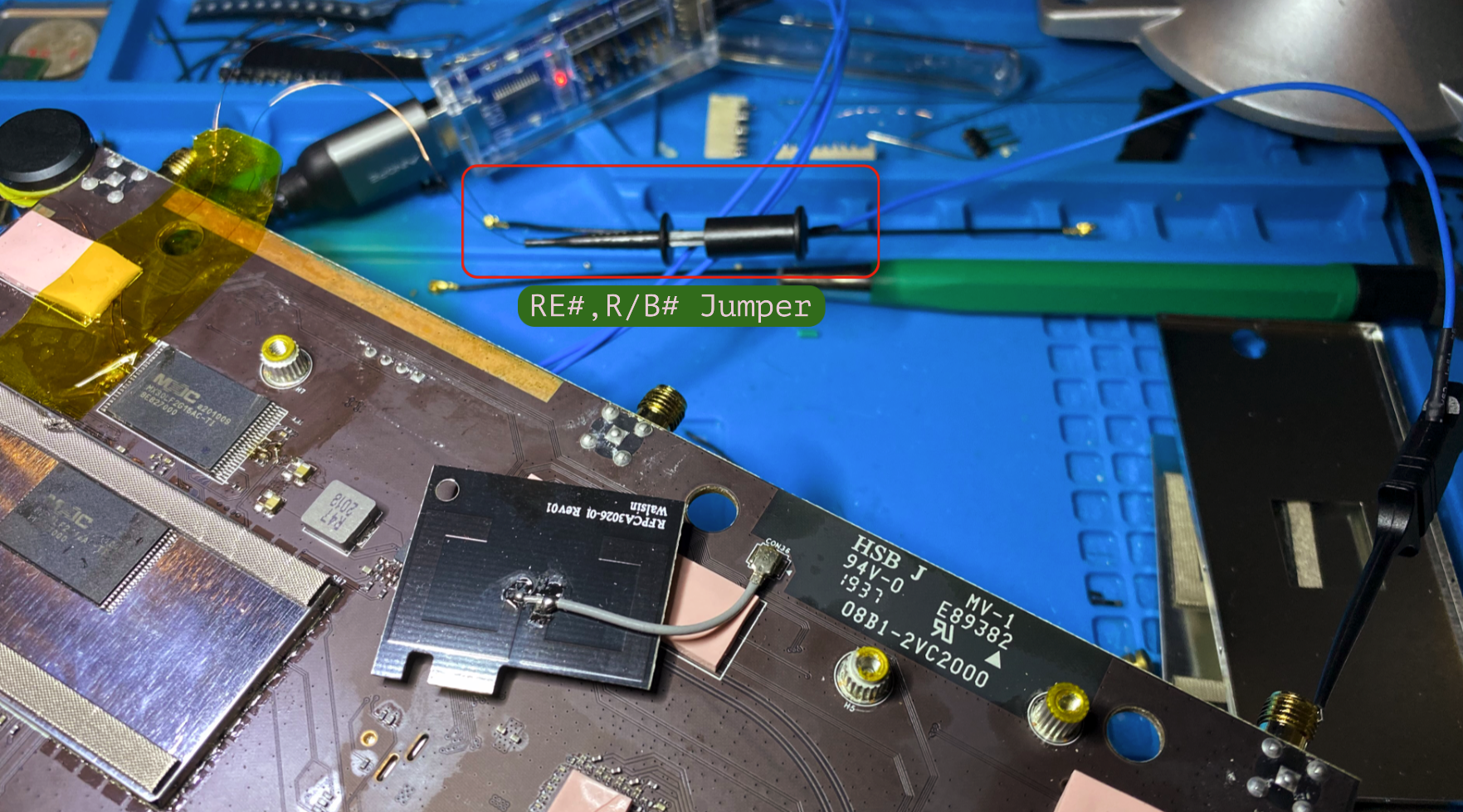
The most likely culprits were the Read Enable (RE#) or Ready/Busy (R/B#) pins changing state. To test this, jumper wires were added to both:
At this point the NAND had to be placed back on the board in order to return the system back to the boot loader, the NAND was once again powered down by disconnecting the VCC jumpers and the RE#,R/B# lines were held low by attaching them to ground:
The NAND was again removed, working one side at a time while monitoring the boot loader console:
This time the boot loader remained active and the system did not reboot. With one more part of the puzzle completed it was time to move on to the next step - attaching the corrupted NAND to the running target.
Once again hot air was used to solder the replacement NAND to the target, the first attempt was unsuccessful as some pins were shorted when trying to get the alignment right on both sides. As encountered previously, failure at this point requires starting the entire process over again - the replacement NAND had to be removed and the original had to be placed back on the board.
For the second attempt, a small piece of paper was used to insulate one side of the NAND while the other was aligned and attached with hot air:
Once the first side was attached, the paper was removed and the other side was attached. The boot loader remained active once the new NAND was in place. The next step was to re-enable the RE#,R/B# pins by removing the ground jumper wires and finally VCC jumper was reattached. Once everything was reconnected, confirmation that the NAND was available was done again with the dn command:
CFE> dn
------------------ block: 0, page: 0 ------------------
00000000: 00000000 00000000 00000000 00000000    ................
00000010: 00000000 00000000 00000000 00000000    ................
00000020: 00000000 00000000 00000000 00000000    ................
<CUT FOR LENGTH>
----------- spare area for block 0, page 0 -----------
00000800: ff851903 20080000 00c2b822 c978ff97    .... ......".x..
00000810: ffffffff ffffffff ffee9423 4ba37819    ...........#K.x.
00000820: ffffffff ffffffff ffee9423 4ba37819    ...........#K.x.
00000830: ffffffff ffffffff ffee9423 4ba37819    ...........#K.x.

*** command status = 1   <----- Success!
CFE>
With a successful test read completed, the factory firmware image was loaded through the boot loader's web interface:
web info: Waiting for connection on socket 1.␛[J
web info: Upload 70647828 bytes, flash image format.␛[J   <----- Image Upload
CFE> ........

Setting JFFS2 sequence number to 13

Flashing root file system at address 0x06000000 (flash offset 0x06000000): <-----Image Write
.................................................................... .....................................................................
....................................................................
....................................................................
....................................................................
....................................................................
....................................................................
....................................................................
Resetting board in 0 seconds...�----
BTRM
V1.6
CPU0
L1CD
MMUI
MMU7
DATA
ZBBS
MAIN
OTP?
OTPP
USBT
NAND
IMG?
IMGL
UHD?
UHDP
RLO?
RLOP
UBI?
UBIP
PASS
----
<CUT FOR LENGTH>
CFE version 1.0.38-161.122 for BCM94908 (64bit,SP,LE)
Build Date: Mon May 13 08:23:21 CST 2019 (defjovi@ubuntu-eva02)
Copyright (C) 2000-2015 Broadcom Corporation.

Boot Strap Register:  0x6fc42
Chip ID: BCM4906_A0, Broadcom B53 Quad Core: 1800MHz
Total Memory: 536870912 bytes (512MB)
Status wait timeout: nandsts=0x50000000 mask=0x40000000, count=0
NAND ECC BCH-4, page size 0x800 bytes, spare size used 64 bytes
NAND flash device: , id 0xc2da block 128KB size 262144KB
<CUT FOR LENGTH>
Initalizing switch low level hardware.
pmc_switch_power_up: Rgmii Tx clock zone1 enable 1 zone2 enable 1.
Software Resetting Switch ... Done.
Waiting MAC port Rx/Tx to be enabled by hardware ...Done
Disable Switch All MAC port Rx/Tx
*** Press any key to stop auto run (1 seconds) ***
Auto run second count down: 0
Booting from only image (address 0x06000000, flash offset 0x06000000) ...  <----- Success!!111!
Decompression LZMA Image OK!
Entry at 0x0000000000080000
Starting program at 0x0000000000080000
/memory = 0x20000000
Booting Linux on physical CPU 0x0
Linux version 4.1.27 (jenkins@asuswrt-build-server) (gcc version 5.3.0 (Buildroot 2016.02) ) #2 SMP PREEMPT Fri Jun 19 13:05:44 CST 2020
CPU: AArch64 Processor [420f1000] revision 0
Detected VIPT I-cache on CPU0
As shown in the output, the flash was successful and the system booted into the target operating system.
I am sure some reading this will say - "why not use $device_name_here chip reader/writer to reprogram the NAND?", which is an absolutely fair question and probably makes more sense than this nonsense; However, I believe the fitting quote to reference here is one by the famous chaos theory mathematician:
'Your scientists were so preoccupied with whether they could, they didn't stop to think if they should'
- Dr. Jeffrey Goldblum